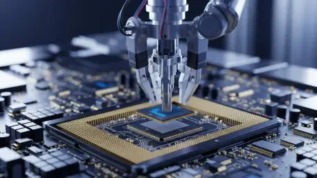

The relentless expansion of digital infrastructure is pushing the global semiconductor market toward a staggering valuation of one point six trillion dollars by the end of the decade, marking a definitive departure from the age of general-purpose processors. This massive shift is not merely about scaling up raw power; it is about a fundamental transformation in how silicon interacts with software. For decades, the Central Processing Unit served as the reliable “jack-of-all-trades” of the technology world, but in an environment dominated by massive artificial intelligence training sets and real-time data streams, that versatility has become a significant liability. The wasted action inherent in general-purpose circuits now represents a drain on energy and efficiency that modern enterprises can no longer afford to ignore.
The $1.6 Trillion Shift: Why General-Purpose Computing Can No Longer Keep Pace
The transition away from standard hardware is driven by the stark reality that traditional chips are struggling to keep up with the exponential growth of artificial intelligence. While Moore’s Law historically provided a predictable path for performance increases, the physical limits of miniaturization have forced designers to look toward architectural efficiency rather than just transistor density. In a landscape where energy consumption and cooling costs dictate the viability of data centers, the broad compatibility of a general-purpose processor is often seen as a burden. These chips spend a significant portion of their energy managing overhead and instructions that are irrelevant to specialized workloads, leading to a performance plateau.
Moreover, the industry has reached a turning point where the efficiency of a single, hardwired task is becoming more valuable than the flexibility to perform multiple tasks with mediocre results. This shift is centered on the Application-Specific Integrated Circuit, or ASIC, which is a specialized tool built for the specific purpose of maximum efficiency. By eliminating the hardware required for unrelated tasks, an ASIC can devote all its resources to one specific algorithm or function. This design philosophy is quickly becoming the standard for any organization handling high-volume data, as it allows for a level of precision that standard logic chips cannot hope to achieve.
From General Versatility to Precision Engineering: The Strategic Importance of Custom Silicon
To understand the strategic necessity of custom silicon, one must look at the physical and economic constraints of the modern tech ecosystem. While standard logic chips like Graphics Processing Units and Neural Processing Units offer significant power for parallel processing, they are still built on platforms designed for broad compatibility. In contrast, an ASIC is stripped of every unnecessary transistor, focusing entirely on a predictable and repetitive workload. This lean architecture is essential because energy consumption and physical space have become the primary bottlenecks for global tech giants. Custom silicon provides a way to bypass these limits by doing more with less, which is why proprietary chip programs have become a hallmark of industry leadership.
Sustainability has also become a major driver in the move toward custom hardware. As massive data centers attempt to reduce their carbon footprints, the energy savings offered by specialized chips provide a clear path to environmental targets. Whether it is a smartphone requiring longer battery life for local machine learning tasks or a server farm trying to optimize heat dissipation, the move toward custom silicon is a pragmatic response to a world where “good enough” performance is no longer sustainable. Consequently, firms that invest in their own silicon are gaining a massive advantage in operational costs, effectively decoupled from the price fluctuations and power limitations of off-the-shelf components.
Decoding the ASIC Landscape: Architecture, Industry Players, and Real-World Applications
The ASIC sector functions as a diverse ecosystem that balances high-performance engineering with economic viability. These chips are generally categorized into three main types based on their design flexibility. Full-custom designs offer the absolute maximum performance because every logic gate is tailored from the ground up, though they come with high development costs. Semi-custom designs utilize pre-existing logic blocks to speed up delivery times, while programmable ASICs allow for adjustments after the manufacturing process is complete. This technical variety allows the hardware to serve as the backbone for several critical industries, from telecommunications and 5G packet routing to the complex signal processing required in modern satellite arrays.
Beyond the data center, ASICs have become integral to the safety and reliability of physical infrastructure. In the automotive industry, Advanced Driver Assistance Systems rely on the millisecond-precision of custom chips to power autonomous driving features and collision avoidance. In the world of finance, the intensive calculations required for cryptocurrency security and high-frequency trading would be impossible without the speed of dedicated logic. This hardware provides reliability in environments where standard chips would fail, including radiation-hardened versions designed specifically for spacecraft. The manufacturing of these chips is a collaborative effort between design powerhouses and specialized foundries like TSMC or Samsung, creating a complex global value chain.
Hardwired for Performance: Expert Insights into the Synergy of AI and Application-Specific Logic
Industry experts from firms like Cadence Design Systems point out that the true value of an ASIC lies in its performance-per-watt metrics. Research into specialized hardware, such as Google’s Tensor Processing Units, shows they can deliver up to 30 times the performance and 80 times the energy efficiency of general-purpose hardware. This is particularly relevant as artificial intelligence models grow in complexity and size, requiring hardware that can handle the specific mathematical operations of neural networks without unnecessary power draw. The frontier of this field is moving toward a concept known as “hardwired AI,” where the software logic is essentially etched directly into the silicon.
By bypassing the traditional bottlenecks where data must constantly travel between a processor and separate memory modules, these hardwired chips offer a radical jump in speed. Pioneers in this space, such as Taalas, are demonstrating that chips can be designed where the logic of the chip is the model itself. This evolution suggests a future where the distinction between software and hardware disappears entirely. Instead of a chip that loads a model into memory, the chip exists as a physical manifestation of the AI, offering processing speeds up to 50 times faster than current industry-standard GPUs. This synergy ensures that as AI continues to evolve, the hardware will not just support it but will define its physical limits.
Assessing the Transition: A Strategic Framework for Custom Silicon Adoption
The transition to specialized computing required a new hierarchy in the technology industry. Companies that prioritized architectural sovereignty secured a dominant position by identifying repetitive high-volume workloads where efficiency gains offset the high initial design costs. The process began with meticulous workload profiling to ensure that a task was stable enough to justify a chip that could not be repurposed. Following this, strategic alliances with specialized foundries allowed organizations to access advanced manufacturing nodes that were previously the exclusive domain of traditional chipmakers. This change turned hardware from a commodity into a core intellectual property asset.
Efficiency auditing became the primary metric for success, measuring the projected performance-per-watt against established benchmarks to validate development costs. Furthermore, the focus shifted toward the edge of the network, where custom silicon reduced latency in critical environments like smart city sensors and autonomous vehicle networks. This transition proved that remote data processing was no longer the only option for high-stakes applications. By integrating these specialized tools, the industry managed to sustain the growth of artificial intelligence while significantly lowering the total cost of ownership. The move toward hardwired logic ultimately established a more sustainable and high-performance foundation for the next decade of digital innovation.